Sunday, August 28, 2022
MFIS finfet

Monday, August 22, 2022
InGaN solar cell
go atlas
set temp=400
set ptype=1e15
set ntype=5e19
set thp=0.3
set thn=0.3
mesh auto
#meshing============================================================
x.m loc=0 spac=.1
x.m loc=1 spac=.1
#
y.m loc=0 spac=.2
y.m loc=0.2 spac=.1
y.m loc=0.2+$thp spac=.1
y.m loc=0.2+$thp+$thn spac=.1
#region============================================================
region num=1 mat=air x.min=0 y.min=0
region num=2 mat=ITO x.min=0 x.max=1 y.min=0 y.max=0.2
region num=3 material=InGaN x.min=0 x.max=1 y.min=0.2 y.max=0.2+$thp acceptor=$ptype
region num=4 material=InGaN x.min=0 x.max=1 y.min=0.2+$thp y.max=0.2+$thp+$thn donor=$ntype
#electrode============================================================
electrode num=1 name=anode x.min=0 x.max=1 y.min=0 y.max=0.2 mat=ITO
electrode num=2 name=cathode x.min=0 x.max=1 y.min=0.2+$thp+$thn y.max=0.2+$thp+$thn material=InGaN
#material============================================================
material material=air real.index=1 imag.index=0
material material=ITO eg300=3.5 affinity=2.3 permittivity=9 NC300=5e17 NV300=5e17 MUN=30 MUP=5 sopra=Ito2.nk taun0=1e-9 taup0=1e-9
material mat=InGaN EG300=1.39 PERMITTIVITY=12.8 AFFINITY=5.4 MUN0=1250 MUP0=650 NC300=5e17 NV300=5e17 taup0=1e-9 taun0=1e-9
#
#beam============================================================
beam num=1 am1.5g x.origin=0.0 y.origin=-2.0 angle=90.0 tr.mat
contact name=anode SURF.REC VSURFN=1e3 VSURFP=1e3
contact name=cathode SURF.REC VSURFN=1e3 VSURFP=1e3
models srh fermi ni.fermi auger optr print
method newton autonr trap maxtrap=10 itlimit=40
#
solve init
solve b1=0.001
solve b1=0.01
solve b1=0.1
solve b1=1
#
log outf=cd.log
solve lambda=0.3 wstep=0.01 wfinal=1.1
log off
extract init infile="cd.log"
extract name="EQE2" curve(elect."optical wavelength",-(i."anode")/elect."source photo current"*) outf="EQE01_1.dat"
tonyplot cd.dat
quit
Sunday, August 21, 2022
NC-FINFET
code:-
go devedit simflags="-3d"
work.area x1=-0.0135 y1=-0.0135 x2=0.0235 y2=0.045
#
#
region reg=1 mat=Silicon color=0xffcc00 pattern=0x4 z1=0.01 z2=0.09 \
polygon="0,0 0.01,0 0.01,0.015 0,0.015"
constr.mesh region=1 default max.height=0.01 max.width=0.02
#
#
region reg=2 name=gate mat=Polysilicon elec.id=1 work.func=0 color=0xffc8c8 pattern=0x7 z1=0.035 z2=0.065 \
polygon="-0.0135,0.015 -0.01,0.015 -0.01,-0.01 0.02,-0.01 0.02,0.015 0.0235,0.015 0.0235,-0.0135 -0.0135,-0.0135 -0.0135,0.015"
constr.mesh region=2 default max.height=0.01 max.width=0.02
#
#
region reg=3 mat="Silicon Oxide" color=0xff pattern=0x2 z1=0.01 z2=0.09 \
polygon="0.013,0.015 0.01,0.015 0.01,0 0,0 0,0.015 -0.003,0.015 -0.003,-0.003 0.013,-0.003"
constr.mesh region=3 default max.height=0.001 max.width=0.001
#
#
region reg=4 name=ferric mat=HfO2 work.func=0 color=0xffff00 pattern=0x5 z1=0.035 z2=0.065 \
polygon="0.0165,-0.0065 -0.0065,-0.0065 -0.0065,0.015 -0.01,0.015 -0.01,-0.01 0.02,-0.01 0.02,0.015 0.0165,0.015"
constr.mesh region=4 default max.height=0.01 max.width=0.02
#
#
region reg=5 mat="Silicon Oxide" color=0xff pattern=0x2 z1=0 z2=0.1 \
polygon="-0.0135,0.015 -0.003,0.015 0,0.015 0.01,0.015 0.013,0.015 0.0235,0.015 0.0235,0.045 -0.0135,0.045"
constr.mesh region=5 default max.height=0.01 max.width=0.02
#
#
region reg=6 name=drain mat=Aluminum elec.id=2 work.func=0 color=0xffc8c8 pattern=0x7 z1=0 z2=0.01 \
polygon="0,0 0.01,0 0.01,0.015 0,0.015"
constr.mesh region=6 default max.height=0.01 max.width=0.02
#
#
region reg=7 name=source mat=Aluminum elec.id=3 work.func=0 color=0xffc8c8 pattern=0x7 z1=0.09 z2=0.1 \
polygon="0,0 0.01,0 0.01,0.015 0,0.015"
constr.mesh region=7 default max.height=0.01 max.width=0.02
#
#
region reg=8 material=Polysilicon work.func=0 color=0xffc8c8 pattern=0x5 z1=0.035 z2=0.065 \
polygon="0.013,-0.003 -0.003,-0.003 -0.003,0.015 -0.0065,0.015 -0.0065,-0.0065 0.0165,-0.0065 0.0165,0.015 0.013,0.015"
constr.mesh region=8 default max.height=0.01 max.width=0.02
#
#
# Set Meshing Parameters
#
base.mesh height=0.01 width=0.005
#
bound.cond !apply max.slope=28 max.ratio=300 rnd.unit=0.0001 line.straightening=1 align.points when=automatic
#
imp.refine min.spacing=0.02 z=0
#
constr.mesh max.angle=90 max.ratio=300 max.height=10000 \
max.width=10000 min.height=0.0001 min.width=0.0001
#
constr.mesh type=Semiconductor default
#
constr.mesh type=Insulator default
#
constr.mesh type=Metal default
#
constr.mesh type=Other default
#
constr.mesh region=1 default max.height=0.01 max.width=0.02
#
constr.mesh region=2 default max.height=0.001 max.width=0.001
#
constr.mesh region=3 default max.height=0.01 max.width=0.02
#
constr.mesh region=4 default max.height=0.01 max.width=0.02
#
constr.mesh region=5 default max.height=0.01 max.width=0.02
#
constr.mesh region=6 default max.height=0.01 max.width=0.02
Mesh Mode=MeshBuild
z.plane z=0 spacing=0.1
z.plane z=0.005 spacing=0.1
z.plane z=0.01 spacing=0.1
z.plane z=0.012 spacing=0.1
z.plane z=0.0167 spacing=0.1
z.plane z=0.0233 spacing=0.1
z.plane z=0.0267 spacing=0.1
z.plane z=0.030 spacing=0.1
z.plane z=0.0315 spacing=0.1
z.plane z=0.033 spacing=0.1
z.plane z=0.035 spacing=0.1
z.plane z=0.041 spacing=0.1
z.plane z=0.047 spacing=0.1
z.plane z=0.053 spacing=0.1
z.plane z=0.059 spacing=0.1
z.plane z=0.065 spacing=0.1
z.plane z=0.067 spacing=0.1
z.plane z=0.0685 spacing=0.1
z.plane z=0.070 spacing=0.1
z.plane z=0.0733 spacing=0.1
z.plane z=0.0767 spacing=0.1
z.plane z=0.0833 spacing=0.1
z.plane z=0.088 spacing=0.1
z.plane z=0.090 spacing=0.1
z.plane z=0.095 spacing=0.1
z.plane z=0.100 spacing=0.1
z.plane max.spacing=1000000 max.ratio=1.5
structure outf=ncfinfet_0.str
go atlas
electrode name=bulk bottom
doping num=1 n.type uniform conc=1e18 reg=6
doping num=2 n.type uniform conc=1e18 reg=7
material material=Silicon eg300=1.1245 affinity=4.05 permitti=11.9
material material=HFO2 ferro.ps=0.5e-6 ferro.pr=0.4e-6 ferro.ec=100000.0 ferro.eps=10.0
material material=Oxide eg300=8.05 affinity=1.00 permittivity=3.9 nc300=2.8e19 nv300=1.04e19
#
contact name=gate workf=5.1
model fermi bqp.n srh ferro hcte.el evsatmod=0 fldmob print
method newton dvlimit=1.0 maxtrap=6
solve init
solve vdrain=0.01
solve vdrain=0.05
solve vdrain=0.1
log outf=ncfinfet.log
solve vgate=0.0 name=gate vstep=0.1 vfinal=1.0
log off
output p.quantum band.temp con.band val.band band.par
save outf=ncfinfet_1.str master
tonyplot ncfinfet.log
tonyplot3d ncfinfet_1.str -set ncfinfet_0.set
tonyplot3d ncfinfet_1.str -set ncfinfet_1.set
extract name="subvt" 1.0/slope(maxslope(curve(v."gate",log10(abs(i."drain")))))
extract name="Ioff_n" y.val from curve(v."gate",i."drain") where x.val=0
extract name="Ion_n" y.val from curve(v."gate",i."drain") where x.val=1
quit
result:-
Sunday, July 24, 2022
DG-MOSFET
code:-
go atlas
set mat=sio2
set vdrain=1.0
mesh space.mult=1.0
#
x.m l=0.00 s=0.5
x.m l=0.07 s=0.001
x.m l=0.075 s=0.0005
x.m l=0.1 s=0.0005
x.m l=0.11 s=0.001
x.m l=0.175 s=0.5
#
y.m l= 0.0 s=.005
y.m l= 0.001 s=0.001
y.m l= 0.0025 s=0.0005
y.m l= 0.0125 s=0.0005
y.m l= 0.014 s=0.001
y.m l= 0.015 s=.005
#
region num=1 x.min=0 y.min =0 mat= air
region num=2 x.min=0.0 x.max=0.075 y.min=0.0025 y.max=0.0125 mat = silicon
region num=3 x.min=0.075 x.max=0.1 y.min=0.0025 y.max=0.0125 mat = silicon
region num=4 x.min=0.1 x.max=0.175 y.min=0.0025 y.max=0.0125 mat = silicon
region num=5 x.min=0.07 x.max=0.11 y.min= 0.001 y.max=0.0025 mat = $mat
region num=6 x.min=0.07 x.max=0.11 y.min= 0.0125 y.max=0.014 mat = $mat
#
electrode num=1 name= source x.min = 0 x.max=0 y.min=0.0025 y.max=0.0125
electrode num=2 name= drain x.min=0.175 x.max=0.175 y.min=0.0025 y.max=0.0125
electrode num=3 name=gate x.min=0.07 x.max=0.11 y.min=0.0 y.max=0.001
electrode num=4 name=gate2 x.min=0.07 x.max=0.11 y.min= 0.014 y.max=0.015
#
doping uniform conc =1E20 n.type region = 2
doping uniform conc =1E17 n.type region = 4
doping uniform conc =1E14 p.type region = 3
#
save outf=abc.str
tonyplot abc.str
#
material material = silicon
#
model conmob srh fldmob bgn fermi print
#
method newton trap maxtrap=5
#
contact name=gate workfun=4.8
contact name=gate2 workfun=4.8 common = gate
contact name=source
contact name=drain
#
solve init
solve prev
solve vdrain = 0.1
solve vdrain = 0.2
solve vdrain = 0.3
solve vdrain = 0.6
solve vdrain = 1.0
solve vdrain = $vdrain
log outf=dgft.log
solve vgate=0 vstep=0.02 vfinal=2 name=gate
output band.param con.band val.band e.mobility ex.velocity ey.velocity e.velocity
tonyplot dgft.log
save outf=abc.str
tonyplot abc.str
Saturday, July 2, 2022
Textured solar cell (Spectral response)
code:---
go athena
#
line x loc=0.00 spac=0.1
line x loc=0.25 spac=0.1
line x loc=0.50 spac=0.1
line x loc=0.75 spac=0.1
line x loc=1.0 spac=0.1
line x loc=1.25 spac=0.1
line x loc=1.5 spac=0.1
line x loc=1.75 spac=0.1
line x loc=2.0 spac=0.1
line x loc=2.125 spac=0.1
#
line y loc=0.00 spac=0.1
line y loc=4.00 spac=0.1
line y loc=8.00 spac=0.1
line y loc=12.00 spac=0.5
line y loc=20.00 spac=2.0
line y loc=24.00 spac=2.0
# doped with phosphorous
init silicon c.phosphor=1.0e15 two.d orientation=100
#ecthing process
etch silicon start x=0 y=0
etch cont x=0.25 y=0
etch cont x=0.5 y=4
etch cont x=0.75 y=4
etch cont x=1 y=0
etch cont x=1.25 y=0
etch cont x=1.5 y=4
etch cont x=1.75 y=4
etch done x=2.0 y=0
struct mirror right
save outf=abc.str
tonyplot abc.str
go atlas
mesh infile=abc.str
electrode num=1 name=anode x.min=0.0 x.max=.25 top mat=silver
electrode num=2 name=anode x.min=1 x.max=1.25 top mat=silver
electrode num=3 name=anode x.min=2 x.max=2.25 top mat=silver
electrode num=4 name=anode x.min=3 x.max=3.25 top mat=silver
electrode num=5 name=anode x.min=4 x.max=4.25 top mat=silver
electrode num=6 name=cathode y.min=24 y.max=24 mat=silver
material material=silicon mun0=1000 mup0=500 eg300=2.0 taun0=1e-6 taup0=1e-6 sopra=Si100_2.nk
beam num=1 am1.5g x.origin=0 y.origin=-1.0 angle=90 wavel.start=0.4 wavel.end=1 wavel.num=100
mat taun0=1e-6 taup0=1e-6
output val.band con.band opt.int
models conmob fldmob srh auger print
method newton autonr trap
contact name=anode workfun=5.1
contact name=cathode
solve init
solve b1=0.001
solve b1=0.01
solve b1=0.1
solve b1=1
log outf=iv.log
solve b1=1 lambda=0.3 wstep=0.01 wfinal=1.0
log off
tonyplot iv.log
extract init infile="iv.log"
extract name="EQE2" curve(elect."optical wavelength",-(i."anode")/elect."source photo current"*elect."Absorption") outf="EQE01_1.dat"
tonyplot EQE01_1.dat
save outf=abc.str
tonyplot abc.str
result:---
Wednesday, April 20, 2022
OFET(Also you can know how to use pentacene and poole frenkel mobility here)
go atlas
mesh space.mult=1
x.m l=0 s=0.5
x.m l=10 s=0.5
x.m l=15 s=0.5
x.m l=20 s=0.5
x.m l=30 s=0.5
y.m l=-0.03 s=0.01
y.m l=0 s=0.005
y.m l=0.015 s=0.003
y.m l=0.03 s=0.005
y.m l=0.0325 s=0.001
y.m l=0.0357 s=0.001
y.m l=0.0557 s=0.0025
region num=1 material=Pentacene x.min=0 x.max=30 y.min=-0.03 y.max=0.03 acceptor=7e17
region num=2 material=Al2O3 x.min=0 x.max=30 y.min=0.03 y.max=0.0357
electrode num=1 name=source x.max=10 y.min=0.0 y.max=0.03 material=Gold
electrode num=2 name=gate x.min=0 x.max=30 y.min=0.0357 y.max=0.0557 material=Aluminium
electrode num=3 name=drain x.min=20 y.min=0.00 y.max=0.03 material=Gold
material material=Pentacene eg300=2.8 nc300=1e21 nv300=1e21 permittivity=4.0
material material=Al2O3 permittivity=4.5
#
mobility region=1 deltaep.pfmob=0.0179 betap.pfmob=7.75e-5 mun=5e-5 mup=0.85
#
models conmob srh fermi print
models region=1 pfmob.p
#
method newton autonr trap
#
contact name=gate workfun=4.6
contact name=source workfun=5.1
contact name=drain workfun=5.1
#
solve init
solve prev
solve vdrain=2.5
log outf=abc0.log
solve vgate=-20 name=gate vstep=1 vfinal=20
tonyplot abc0.log
output val.band con.band band.param
save outf=abc.str
tonyplot abc.str
Thursday, April 7, 2022
Tunnel field effect transistor -VTFET
go atlas
mesh auto
#
x.mesh loc=0 spac=0.1
x.mesh loc=.002 spac=.001
x.mesh loc=.004 spac=.001
x.mesh loc=.005 spac=.005
x.mesh loc=.007 spac=.0001
x.mesh loc=.017 spac=.0001
x.mesh loc=.019 spac=.005
x.mesh loc=.020 spac=.001
x.mesh loc=.022 spac=.001
x.mesh loc=.024 spac=0.1
#
y.mesh loc=0 spac=.005
y.mesh loc=.010 spac=.001
y.mesh loc=.018 spac=.001
y.mesh loc=.022 spac=.001
y.mesh loc=.040 spac=.0001
y.mesh loc=.042 spac=.0001
y.mesh loc=.060 spac=.0005
y.mesh loc=.061 spac=.0005
y.mesh loc=.079 spac=.005
#
region num=1 material=air x.min=0 y.min=0
region num=2 material=silicon x.min=.007 x.max=.017 y.min=.001 y.max=.021
region num=3 material=silicon x.min=.007 x.max=.017 y.min=.021 y.max=.041
region num=4 material=silicon x.min=.007 x.max=.017 y.min=.041 y.max=.061
region num=5 material=silicon x.min=0 x.max=.024 y.min=.061 y.max=.081
region num=6 material=hfo2 x.min=0.005 x.max=.007 y.min=.021 y.max=.041
region num=7 material=hfo2 x.min=0.017 x.max=.019 y.min=.021 y.max=.041
#
qtx.mesh loc=0.005 spac=0.01
qtx.mesh loc=0.020 spac=0.001
qtx.mesh loc=0.019 spac=0.001
qtx.mesh loc=0.022 spac=0.01
#
qty.mesh loc=0.002 spac=0.005
qty.mesh loc=0.003 spac=0.0005
qty.mesh loc=0.045 spac=0.0005
qty.mesh loc=0.055 spac=0.0005
#
electrode name=gate x.min=.003 x.max=.005 y.min=.021 y.max=.041
electrode name=gate2 x.min=.019 x.max=.021 y.min=.021 y.max=.041
electrode name=source x.min=.007 x.max=.017 y.min=0 y.max=0.001
electrode name=drain x.min=0 x.max=.007 y.min=0.059 y.max=0.061
electrode name=drain2 x.min=.017 x.max=.024 y.min=0.059 y.max=0.061
#
material material=silicon me.tunnel=.24 mh.tunnel=.20
#
doping uniform p.type conc=2e19 reg=2
doping uniform p.type conc=5e16 reg=3
doping uniform n.type conc=5e18 reg=4
#
models bbt.nonlocal qtunn.dir=0 bgn srh ni.fermi conmob cvt print temp=300
#
contact name=gate workfun=4.2
contact name=gate2 workfun=4.2 common=gate
contact name=source
contact name=drain
contact name=drain2 common=drain
save outf= abc.str
tonyplot abc.str
#
#
method newton autonr trap maxtrap=10
#solve
solve init
solve prev
solve vdrain=0.1
solve vdrain=0.5
solve vgate=-.3
solve vgate=-.2
log outf=tfet.log
solve name=gate vgate=-0.2 vstep=0.05 vfinal=2.0
tonyplot tfet.log
output val.band con.band qfn qfp e.field j.electron j.hole j.conduction j.total
save outf= abc.str
tonyplot abc.str
quit
result:-
Sunday, March 6, 2022
Amorphous solar cell
code:-
go atlas
mesh auto
#
x.mesh loc=0.0 spacing=0.1
x.mesh loc=1.0 spacing=0.1
region material=Silicon bot ny=50 thick=0.5
#
elec num=1 name=anode y.max=0.05 material=ITO
elec num=2 name=cathode y.min=0.45 y.max=0.5 material=Ito
doping uniform conc=1e12 n.type
doping gaus peak=0.05 char=0.01 conc=1e16 p.type dir=y
doping gaus peak=0.45 char=0.01 conc=1e16 n.type dir=y
material mat=Silicon mun=20 mup=1.5 nc300=2.5e18 nv300=1.9e19 eg300=1.9
defects mat=silicon nta=1.e19 ntd=1.e19 wta=0.033 wtd=0.049 \
nga=1.5e15 ngd=1.5e15 ega=0.62 egd=0.78 wga=0.15 wgd=0.15 \
sigtae=1.e-16 sigtah=1.e-15 sigtde=1.e-15 sigtdh=1.e-16 \
siggae=2.e-16 siggah=2.e-15 siggde=2.e-15 siggdh=2.e-16 \
continuous
material mat=ITO sopra=Ito2.nk
models srh auger fermi ni.fermi conmob print
method newton trap
beam num=1 am1.5g x.o=0 y.o=-1.0 angle=90 tr.mat
save outf=abc.str
tonyplot abc.str
solve init
solve b1=1.0
log outf=abc.log
solve vanode=0.0 name=anode vstep=0.01 vfinal=1.2
tonyplot abc.log
extract init infile="abc.log"
extract name="Jsc" max(curve(v."anode", i."cathode")) outf="I.log"
extract name="JscmAcm2" $Jsc*1e08*1e03 outf="J.dat"
extract name="Voc" x.val from curve(v."anode",i."cathode") where y.val=0.0 outf="V.dat"
extract name="Pm" max(curve(v."anode", (v."anode" *i."cathode"*(-1))))
extract name="FF" ($"Pm"/($"Jsc"*$"Voc"))*100
extract name="Opt_int" max(beam."1")
extract name="Eff" (1e8*$Pm/$Opt_int)*100 outf="E.dat"
quit
Result:-
pervoskite solar cell
All the contents are free
silvaco code:-
go atlas
mesh space.mult=1
x.m l=0.0 s=.05
x.m l=1.0 s=.05
y.m l=0 s=0.01
y.m l=0.135 s=.01
y.m l=0.455 s=.02
y.m l=0.525 s=.02
y.m l=0.550 s=.1
region num=1 mat=air x.min=0 y.min=0
region num=2 mat=ITO x.min=0 x.max=1.0 y.min=0 y.max=0.055
region num=3 user.material=NiO x.min=0 x.max=1.0 y.min=0.055 y.max=0.135
region num=4 user.material=pervoskite x.min=0 x.max=1.0 y.min=.135 y.max=.455
region num=5 material=ZnO x.min=0 x.max=1.0 y.min=.455 y.max=0.525
elec num=1 name=anode x.min=0.0 x.max=1.0 y.min=0 y.max=0.055 mat=ITO
elec num=2 name=cathode x.min=0 x.max=1.0 y.min=0.525 y.max=0.550 mat=aluminium
doping uniform p.type conc=2e16 reg=2
doping uniform p.type conc=5.6e16 reg=3
doping uniform n.type conc=1e15 reg=4
doping uniform n.type conc=1e16 reg=5
material material=air real.index=1.0 imag.index=0
material material=ITO eg300=3.5 affinity=2.3 permittivity=9 NC300=2.2e18 NV300=1.8e19 MUN=30 MUP=5 sopra=Ito2.nk taun0=1e-7 taup0=1e-7
material material=NiO eg300=3.5 affinity=2.2 permittivity=9 NC300=2.2e18 NV300=1.8e19 MUN=4.7 MUP=4.7 \
user.group=semiconductor user.default=sio2 sopra=Tio2b.nk taun0=1e-7 taup0=1e-7
material name=pervoskite eg300=1.55 affinity=3.93 permittivity=10.0 NC300=2.2e18 NV300=1.8e19 MUN=2 MUP=2 sopra=pervoskite.nk taun0=1e-7 taup0=1e-7 \
user.group=semiconductor user.default=GaN
material material=ZnO eg300=3.2 affinity=4 permittivity=8.5 NC300=2.2e18 NV300=1.8e19 MUN=100 MUP=30 sopra=ito2.nk \
taun0=1e-7 taup0=1e-7
#
save outf= struc.str
tonyplot struc.str
beam num=1 am1.5g x.o=0 y.o=-1 angle=90
models srh fermi ni.fermi optr auger bgn print
method newton autonr trap maxtrap=10
output con.band val.band band.par e.mobility e.velocity
contact name=anode workf=5.75
contact name=cathode reflect=0.5 workf=4.7
solve init
solve prev
solve b1=1
log outf=illumination.log
solve name=anode vanode=0 vstep=0.01 vfinal=0.6
log off
tonyplot illumination.log
extract init infile="illumination.log"
extract name="Jsc" max(curve(v."anode", i."cathode")) outf="I.log"
extract name="JscmAcm2" $Jsc*1e08*1e03 outf="J.dat"
extract name="Voc" x.val from curve(v."anode",i."cathode") where y.val=0.0 outf="V.dat"
extract name="Pm" max(curve(v."anode", (v."anode" *i."cathode"*(-1))))
extract name="FF" ($"Pm"/($"Jsc"*$"Voc"))*100
extract name="Opt_int" max(beam."1")
extract name="Eff" (1e8*$Pm/$Opt_int)*100 outf="E.dat"
extract name="Power" curve(v."anode", (v."anode" * i."anode" *(-1))) outf="P.dat"
quit
result:-
Sunday, January 23, 2022
heterojunction bipolar transistor
code:-
go atlas
mesh space.mult=1.0
#
x.mesh loc=0.00 spac=0.25
x.mesh loc=2.00 spac=0.25
x.mesh loc=3.00 spac=0.2
x.mesh loc=4.00 spac=0.2
#
y.mesh loc=0.00 spac=0.03
y.mesh loc=0.15 spac=0.005
y.mesh loc=0.20 spac=0.015
y.mesh loc=0.25 spac=0.01
y.mesh loc=0.50 spac=0.05
y.mesh loc=0.75 spac=0.01
y.mesh loc=0.90 spac=0.03
#
#
region num=1 material=GaAs y.min=0.75
region num=2 material=GaAs y.min=0.25 y.max=0.75
region num=3 material=AlGaAs y.max=0.0 x.comp=0.3 \
grad.34=0.15
region num=4 material=GaAs y.min=0.15 y.max=0.25
region num=5 material=SiO2 y.max=0.15 x.max=3.0
#
elec num=1 name=emitter x.min=3.0 x.max=4.0 y.min=0.0 y.max=0.0
elec num=2 name=base x.min=0.0 x.max=2.0 y.min=0.15 y.max=0.15
elec num=3 name=collector bot
#
doping uniform region=1 n.type conc=2.e17
doping uniform region=2 n.type conc=5.e16
doping uniform region=3 n.type conc=2.e17
doping uniform region=4 p.type conc=2.e18
#
material taun0=1.e-9 taup0=1.e-9
material material=AlGaAs mun=2200 mup=350
model srh fldmob print optr
model material=GaAs conmob evsatmod=1
#
solve init
save outf=hbt.str
tonyplot hbt.str
method gummel newton trap vsatmod.inc=0.01
solve
solve local vcollector=2.0
log outf=hbt.log
solve vbase=0.025
solve vbase=0.1
method newton autonr trap vsatmod.inc=0.01 itlim=50
solve vbase=0.2 vstep=0.1 name=base vfinal=1.4
solve vbase=1.45 vstep=0.025 name=base vfinal=1.5
tonyplot hbt.log
quit
Thursday, January 13, 2022
PIN photodiode
go atlas
mesh space.mult=4.0
#
x.mesh loc=0.0 spacing=0.25
x.mesh loc=10.0 spacing=0.25
#
y.mesh loc=0.0 spacing=0.05
y.mesh loc=5.0 spacing=0.2
y.mesh loc=10.0 spacing=0.05
#
#
region num=1 material=Silicon
#
elec num=1 name=anode x.min=0.0 x.max=10.0 y.max=0.0
elec num=2 name=cathode bottom
#
doping uniform conc=1e14 n.type
doping gaus peak=0.0 char=0.1 conc=1e18 p.type dir=y
doping gaus peak=10.0 char=0.1 conc=1e18 n.type dir=y
#
#
material taup0=2.e-6 taun0=2.e-6
models srh auger conmob fldmob
#
#
save outf=abc.str
tonyplot abc.str
#
#
beam num=1 x.origin=5.0 y.origin=-1.0 angle=90.0 wavelength=.1
#
method newton trap
solve init
solve vcathode=0.2
#
#
log outf=abc.log master
solve prev b1=1 lambda=0.1
solve prev b1=1 lambda=0.2
solve prev b1=1 lambda=0.3
solve prev b1=1 lambda=0.4
solve prev b1=1 lambda=0.5
solve prev b1=1 lambda=0.6
solve prev b1=1 lambda=0.7
solve prev b1=1 lambda=0.8
tonyplot abc.log
quit
Result:-
Friday, December 31, 2021
single-active-layer TFT
silvaco code:-
go atlas
mesh width=100 outf=tft_IGZO.str
x.m l=0 s=1
x.m l=4 s=0.1
x.m l=26 s=0.1
x.m l=30 s=1
#=====================================
y.m l=0 s=0.002
y.m l=0.03 s=0.0005
y.m l=0.13 s=0.010
#=====================================
region num=1 material=igzo y.min=0.000 y.max=0.030
region num=2 material=sio2 y.min=0.030 y.max=0.130
#=====================================
elec num=1 name=gate bottom
elec num=2 name=source y.max=0.0 x.min=0.0 x.max=5
elec num=3 name=drain y.max=0.0 x.min=25 x.max=30
#=====================================
contact num=1 p.poly
contact num=2 workf=4.16
contact num=3 workf=4.16
#=====================================
material region=1 eg300=3.20 mun=15 affinity=4.16 permit=10 nc300=5e18 nv300=3e19
models fermi print
#=====================================
defects nta=1.21e20 ntd=1.55e20 wta=0.030 wtd=0.110 \
ngd=1e16 egd=2.95 wgd=0.1 \
nga=3.2e17 ega=2.0 wga=0.1 \
dfile=IGZO_bulk_don.dat afile=IGZO_bulk_acc.dat continuous numa=200 numd=200
#=====================================
intdefects intnumber=1/2 nta=0 ntd=0 wta=0 wtd=0 \
ngd=6.0e11 egd=2.95 wgd=0.1 nga=0 ega=0 wga=0 \
dfile=IGZO_int_don.dat afile=IGZO_int_acc.dat continuous numa=200 numd=200
#=====================================
output con.band val.band
probe name=my_fermi_front x=15 y=0.0298 QFN
probe name=my_con_front x=15 y=0.0298 CON.BAND
probe name=my_con_back x=15 y=0.0 CON.BAND
#=====================================
solve init
save outf=tftIGZO_init.str
#=====================================
solve vdrain=0 vstep=0.1 vfinal=0.5 name=drain
save outf=tftIGZO_D05V.str
tonyplot tftIGZO_D05V.str
#=====================================
log outf=tftIGZO_neg.log
solve vgate=0 vstep=-0.1 vfinal=-5 name=gate
solve vstep=-0.2 vfinal=-10 name=gate
tonyplot tftIGZO_neg.log
#=====================================
save outf=tftIGZO_negG10V.str
log off
load inf=tftIGZO_D05V.str master
solve prev
log outf=tftIGZO_pos.log
solve vstep=0.1 vfinal=5 name=gate
solve vstep=0.2 vfinal=20 name=gate
tonyplot tftIGZO_neg.log
log off
quit
result:-
BIO TFT
go atlas
mesh width=100 outf=tft_BIO.str
x.m l=0 s=1
x.m l=4 s=0.1
x.m l=26 s=0.1
x.m l=30 s=1
#======================================
y.m l=0 s=0.01
y.m l=0.05 s=0.01
y.m l=0.15 s=0.50
#======================================
region num=1 material=igzo y.min=0 y.max=0.05
region num=2 material=sio2 y.min=0.05 y.max=0.15
#======================
===========
elec num=1 name=gate bottom
elec num=2 name=source y.max=0.0 x.min=0.0 x.max=5
elec num=3 name=drain y.max=0.0 x.min=25 x.max=30
#======================================
contact num=1 p.poly
contact num=2 workf=4.16
contact num=3 workf=4.16
#======================================
material material=igzo eg300=3.2 mun=12
models fermi print
#======================================
defects nta=4e20 ntd=1.55e20 wta=0.057 wtd=0.110 \
ngd=4e18 egd=3.00 wgd=0.14 \
nga=5.57e18 ega=2.0 wga=0.14 \
sigtae=1e-15 sigtah=1e-15 sigtde=1e-15 sigtdh=1e-15 \
siggae=1e-15 siggah=1e-15 siggde=1e-15 siggdh=1e-15 \
dfile=BIO_don.dat afile=BIO_acc.dat continuous numa=200 numd=200
#======================================
solve init
solve vdrain=0.1
save outf=tft_BIO_D01V.str
tonyplot tft_BIO_D01V.str
#======================================
log outf=tft_BIO_neg.log
solve vgate=0 vstep=-.5 vfinal=-10 name=gate
log off
load inf=tft_BIO_D01V.str master
solve prev
log outf=tft_BIO_pos.log
solve vstep=1 vfinal=30 name=gate
log off
#======================================
tonyplot tft_BIO_neg.log -overlay tft_BIO_pos.log
quit
result:-
Monday, December 20, 2021
high-k gate dielectric MISFET
silvaco tcad:
go atlas
#
mesh auto
x.m l=0.00 s=0.1
x.m l=0.8 s=0.05
x.m l=1.3 s=0.1
x.m l=1.8 s=0.05
x.m l=2.6 s=0.1
#
y.m l=-0.004888 s=0.001
y.m l=0.0 s=0.001
y.m l=0.1 s=0.025
y.m l=1 s=0.2
#
region num=1 y.min=0 y.max=1 silicon
region num=2 y.max=0 material=HfO2
electrode name=gate x.min=0.6 x.max=2.0 y.max=-0.004888
electrode name=source x.max=0.5 y.min=0 y.max=0
electrode name=drain x.min=2.1 y.min=0 y.max=0
electrode substrate
doping uniform conc=4e15 p.type
doping gauss n.type conc=1e20 char=0.075 lat.char=0.05 reg=1 x.r=0.6
doping gauss n.type conc=1e20 char=0.075 lat.char=0.05 reg=1 x.l=2
#
#
contact name=gate aluminum
#
mobility rps.n rps.p mun0=5000
#
method newton trap carriers=2
#
solve init
solve vdrain=0.1
#
save outf=high.str
probe name=Eperp x=1.3 y=0.0001 dir=90 field
probe name=charge x.min=1.1 x.max=1.5 n.conc integrate y.min=0 y.max=0.2
#
log outf=highk.log
solve vstep=0.01 name=gate vfinal=2.0
#
tonyplot highk.log
tonyplot high.str
#
quit
result:-
DGMOSFET(double gate MOSFET)
go atlas
mesh space.mult=1.0
#
x.m l=0.00 s=0.05
x.m l=0.001 s=0.001
x.m l=0.003 s=0.0005
x.m l=0.013 s=0.0005
x.m l=0.015 s=0.001
x.m l=0.016 s=0.05
#
y.m l= 0.0 s=.005
y.m l= 0.001 s=0.0005
y.m l= 0.003 s=0.00005
y.m l= 0.007 s=0.00005
y.m l= 0.009 s=0.0005
y.m l= 0.010 s=.005
#
region num=1 x.min=0 y.min =0 mat= air
region num=2 x.min=0.0 x.max=0.003 y.min= 0.003 y.max=0.007 mat = silicon
region num=3 x.min=0.003 x.max=0.013 y.min= 0.003 y.max=0.007 mat = silicon
region num=4 x.min=0.013 x.max=0.016 y.min= 0.003 y.max=0.007 mat = silicon
region num=5 x.min=0.003 x.max=0.013 y.min= 0.001 y.max=0.003 mat = sio2
region num=6 x.min=0.003 x.max=0.013 y.min= 0.007 y.max=0.009 mat = sio2
#
electrode num=1 name= source x.min = 0 x.max=0 y.min=0.003 y.max=0.007
electrode num=2 name= drain x.min = 0.013 x.max=0.013 y.min=0.003 y.max=0.007
electrode num=3 name=gate x.min=0.003 x.max=0.013 y.min=0.0 y.max=0.001
electrode num=4 name=gate2 x.min=0.003 x.max=0.013 y.min= 0.009 y.max=0.010
#
doping uniform conc =2E20 n.type region = 2
doping uniform conc =2E20 n.type region = 4
doping uniform conc =1E18 p.type region = 3
#
#material material = sio2
material material = silicon EG300=1.08 NC300=2.8e19 NV300=1.04e19 PERMITTIVITY=11.8 MUN=2360 AFFINITY=4.284
#
model conmob srh fldmob bgn fermi print
#
method newton trap maxtrap=5
#
contact name = gate workfun = 4.6
contact name = gate2 workfun = 4.6 common = gate
contact name = source
contact name = drain
#
solve init
solve prev
solve vgate = 0.1
solve vgate = 0.2
solve vgate = 0.3
solve vgate = 0.6
solve vgate = 0.8
log outf = dgft.log
solve vdrain = 0 vstep = 0.01 vfinal = 0.7 name = drain
output band.param con.band val.band e.mobility ex.velocity ey.velocity e.velocity
tonyplot dgft.log
save outf=abc.str
tonyplot abc.str
#########################################################################################################
result:-------------------------
Saturday, November 20, 2021
TFET(Basic structure)
silvaco code:-
go atlas
mesh space.mult=0.01
#
x.mesh loc=0 spac=.005
x.mesh loc=.001 spac=.0005
x.mesh loc=.01 spac=.005
x.mesh loc=.03 spac=.005
x.mesh loc=.039 spac=.0005
x.mesh loc=.040 spac=.005
#
y.mesh loc=0 spac=.00005
y.mesh loc=.001 spac=.0005
y.mesh loc=.003 spac=.0005
y.mesh loc=.013 spac=.0005
y.mesh loc=.015 spac=.0005
y.mesh loc=.016 spac=.00005
# region
region num=1 material=air x.min=0 y.min=0
region num=2 material=silicon x.min=0.001 x.max=.01 y.min=.003 y.max=.013
region num=3 material=silicon x.min=.01 x.max=.03 y.min=.003 y.max=.013
region num=4 material=silicon x.min=.03 x.max=.039 y.min=.003 y.max=.013
region num=5 material=HfO2 x.min=0.01 x.max=.03 y.min=.001 y.max=.003
region num=6 material=HfO2 x.min=0.01 x.max=.03 y.min=.013 y.max=.015
#
qtx.mesh loc=0.002 spac=0.001
qtx.mesh loc=0.01 spac=0.0005
qtx.mesh loc=0.024 spac=0.0005
qtx.mesh loc=0.03 spac=0.0005
qtx.mesh loc=0.035 spac=0.001
qty.mesh loc=0.00 spac=0.0005
qty.mesh loc=0.0022 spac=0.0005
qty.mesh loc=0.003 spac=0.0005
qty.mesh loc=0.008 spac=0.0005
qty.mesh loc=0.012 spac=0.005
#electrode
electrode name=gate x.min=.01 x.max=.03 y.min=0 y.max=.001 mat=aluminium
electrode name=gate2 x.min=.01 x.max=.03 y.min=.015 y.max=.016 mat=aluminium
electrode name=drain x.min=0 x.max=0.001 y.min=0.003 y.max=0.013
electrode name=source x.min=.039 x.max=.04 y.min=0.003 y.max=0.013
#
MATERIAL MATERIAL=silicon me.tunnel=.44 mh.tunnel=.52 NC300=1e17 NV300=1e17
material material=hfo2 permittivity=22
#
doping uniform conc=1e20 reg=2
doping uniform conc=5e18 reg=4
#contact
contact name=gate workfun=4.5
contact name=gate2 workfun=4.5 common=gate
contact name=drain workfun=3.9
contact name=source workfun=5.93
save outf=tfet.str
tonyplot tfet.str
#model
models bbt.nonlocal bbt.forward bgn srh auger conmob fldmob cvt print
#
output val.band con.band qfn qfp e.field j.electron j.hole j.conduction j.total
#method
method newton autonr trap maxtrap=10
#solve
solve init
solve prev
solve vdrain=0.0
solve vdrain=0.01
solve vdrain=0.02
solve vdrain=0.03
solve vdrain=0.04
solve vdrain=0.05
log outf=tfet.log
solve name=gate vgate=0 vstep=0.05 vfinal=1.5
tonyplot tfet.log
quit
result:-
Thursday, October 21, 2021
(updated) quantum well solar cell (improved)
Code:-
go atlas
mesh auto
#==================================================================
x.mesh loc=0 s=1
x.mesh loc=400 s=1
#==================================================================
y.mesh loc=0 s=.1
y.mesh loc=0.5 s=.1
y.mesh loc=1.5 s=.1
y.mesh loc=2.0 s=.1
y.mesh loc=2.3 s=.1
#==================================================================
region num=1 material=Si x.min=0 x.max=400 y.min=0 y.max=0.5 acceptor=5e18
region num=2 material=Si x.min=0 x.max=400 y.min=.5 y.max=1.5
region num=3 material=Si x.min=0 x.max=400 y.min=1.50 y.max=2.0 donor=5e18
region num=4 material=Si x.min=0 x.max=400 y.min=2.0 y.max=2.3 donor=5e18
#==================================================================
electrode name=anode top
electrode name=cathode bottom
#==================================================================
material material=Si EG300=1.1 PERMITTIVITY=11.8 AFFINITY=4.07 MUN=1000 MUP=500 NC300=2.8e19 taun0=1e-6 taup0=1e-6 NV300=1.04e19 sopra=Si111.nk
#==========================================================================================================
doping n.type uniform region=4 resisti=0.05
#==================================================================
save outf=usPIN.str
tonyplot usPIN.str
beam num=1 x.o=100 y.o=-2 angle=90 power.file=C:/sedatools/examples/solar/solarex01.spec
output opt.int
#==================================================================
models conmob fermi optr consrh print
method newton autonr trap maxtrap=10
#==================================================================
contact name=anode
contact name=cathode
#==================================================================
#
solve init
solve prev
solve b1=1e-02
solve b1=1e-01
solve b1=1
#==================================================================
log outf=IsPIN.log
solve vanode=0 name=anode vstep=0.3 vfinal=0.6
tonyplot IsPIN.log
#==================================================================
extract init inf="IsPIN.log"
extract name="Jsc" max(curve(v."anode", i."cathode"))
extract name="JscmAcm2" $Jsc*1e08*1e03
extract name="Voc" x.val from curve(v."anode",i."cathode") where y.val=0.0
extract name="Pm" max(curve(v."anode",(v."anode" *i."cathode")))
extract name="Vm" x.val from curve(v."anode",(v."anode"*i."cathode") ) where y.val=$"Pm"
extract name="Im" $"Pm"/$"Vm"
extract name="FF" ($"Pm"/($"Jsc"*$"Voc"))*100
extract name="Eff" (1e8*$Pm/$Opt_int)*100
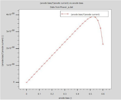
extract name="Power" curve(v."anode", (v."anode" * i."anode" *(-1))) outf="Power_a.dat"
tonyplot Power_a.dat
solve init
solve prev
solve prev b1=0
log outf=solar_0.log
solve b1=1 beam=1 lambda=0.2 wstep=0.02 wfinal=2.0
extract init inf="solar_0.log"
extract name="EQE1" curve(elect."optical wavelength", -(i."anode")/elect."source photo current") outf="EQE1.dat"
tonyplot EQE1.dat
quit
Result:-
telegram me at t.me/KST1729 if you need any help (sorry for older one this is new one)
sorry for older one this is new one
-
silvaco code:- go atlas mesh space.mult=0.01 # x.mesh loc=0 spac=.005 x.mesh loc=.001 spac=.0005 x.mesh loc=.01 spac=.005 x.mesh loc=.03 sp...
-
why we need TFET? TFET are attracting wide attention because of their low subthreshold swing and low OFF-state leakage current . Since the c...
-
sorry for older one this is new one